作者:Ashish Kumar, Raj Kumar Kokkonda, Subhashish Bhattacharya , Victor Veliadis
单位:Dept. of Electrical and Computer Engineering
North Carolina State University
Raleigh, NC, USA
Abstract——Power modules are connected in series and parallel combinations to meet the voltage and current requirements of various applications, especially in medium voltage high power applications. Avalanche ruggedness of the SiC power MOSFETs need to be established in these connections to assess the reliability of the converters in extreme transient conditions. 1700V SiC MOSFET has potential to replace the conventional 1700V silicon IGBT in medium voltage power converters such as 800V and 1500V railway traction applications. In this paper, single shot avalanche ruggedness of the series-connected and parallel-connected 1700V SiC MOSFETs are characterized using the unclamped inductive test circuit. Single shot avalanche ruggedness of series connected SiC MOSFETs is reported for the first time. In both the connections, the failed MOSFET was observed to be the one which dissipated lower share of the total avalanche energy of the connection.
摘要——电源模块采用串联和并联组合方式连接,以满足各种应用对电压和电流的要求,特别是在中压大功率应用中。需要在这些连接中建立SiC功率MOSFET的雪崩坚固性,以评估转换器在极端瞬态条件下的可靠性。1700V SiC MOSFET有潜力取代传统的1700V硅IGBT中压功率变换器,如800V和1500V铁路牵引应用。本文采用无箝位电感测试电路,对1700 V SiC MOSFET串联和并联的单次雪崩坚固性进行了测试。本文首次报道了串联SiC MOSFET的单次雪崩坚固性。在这两种连接中,观察到失效的MOSFET消耗了连接总雪崩能量的较低份额。
Keywords——medium voltage, silicon carbide, avalanche ruggedness, UIS, single shot, SiC MOSFET
关键词——中压,碳化硅,雪崩坚固性,UIS,单次,SiC MOSFET
Ⅰ. Introduction
Silicon carbide (SiC) power devices have received much attention in the last two decades for medium voltage (MV) power applications, such as high speed motor drives, solid state transformers, railway traction and fast chargers for electric vehicles [1]. In medium voltage power converters, typically parallel and series connections of high voltage silicon IGBTs are employed to meet the high voltage and high current requirements. Series connection of power devices are typically used when the high voltage rated devices are not available. Moreover, with a N-fold increase in the voltage rating of SiC power MOSFETs, the on-state resistance of the drift region increases approximately by a factor of N2.5.Therefore, it is preferred to connect SiC MOSFETs in series in order to reduce total conduction losses of the series string, even though it may result in additional switching losses due to the voltage balance requirements. Series connection of 1.7kV and 10kV SiC MOSFETs have been demonstrated earlier in MV power converters [2], [3], [4]. Parallel connection of power modules are usually required when the current rating of the individual module does not meet the total current requirement. Parallel operation needs special current balancing circuit to mitigate static and dynamic current imbalance among the modules due to inherent mismatch in the output characteristics and the circuit layout. Dedicated current balancing techniques for SiC power MOSFET modules have been reported earlier in [5], [6].
在过去二十年中,碳化硅(SiC)功率器件在中压(MV)功率应用中受到了广泛关注,如高速电机驱动、固态变压器、铁路牵引和电动汽车快速充电器[1]。在中压功率变换器中,通常采用高压硅IGBT并联和串联的方式来满足高压大电流的要求。在没有高额定电压设备时,通常采用电源设备的串联连接。此外,随着SiC功率MOSFET的额定电压增加n倍,漂移区的导通电阻大约增加了N2.5倍。因此,为了减少串联串的总导通损耗,最好将SiC MOSFET串联起来,尽管由于电压平衡的要求,可能会导致额外的开关损耗。1.7kV和10kV SiC MOSFET的串联连接早前已在中压功率变换器中得到演示[2],[3],[4]。当单个模块的额定电流不满足总电流要求时,通常需要并联电源模块。并联运行需要特殊的电流平衡电路,以缓解由于输出特性和电路布局的固有不匹配而导致的模块间静态和动态电流不平衡。SiC功率MOSFET模块的专用电流平衡技术已经在[5],[6]中有所报道。
Short circuit and avalanche characteristics of the power MOSFET are two important parameters, which are used to establish the reliability of the power converter in extreme transient conditions. A power MOSFET can be characterized for avalanche ruggedness in single shot operation or repetitive operation. When SiC MOSFETs are operated in series or parallel connections, that combination must be characterized for its avalanche ruggedness. This research focuses on the single shot avalanche characterization of these two combinations of the SiC power MOSFETs.
功率MOSFET的短路和雪崩特性是决定功率变换器在极端瞬态条件下可靠性的两个重要参数。功率MOSFET在单次或重复操作中具有雪崩坚固性。当SiC MOSFET以串联或并联方式工作时,这种组合必须具有雪崩坚固性。本文主要研究了这两种SiC功率MOSFET组合的单次雪崩特性。
800 V dc bus based systems are traditionally used in railway traction applications. Recently, 800 V system has been proposed for the fast chargers in electric vehicle applications. 1700 V SiC MOSFETs have potential to replace the conventional 1700 V silicon IGBTs in these 800 V dc systems. Few railway applications also have 1500 V dc rail systems, where series connection of 1700 V SiC MOSFETs can be used to meet the voltage requirement. In most of these high power applications, parallel connection of the 1700 V MOSFET modules are required to meet the high current requirement. Avalanche ruggedness of 1700 V SiC MOSFETs have been reported for single module operation in [4], [7]. Considerations in parallel connection of low voltage silicon MOSFETs have been discussed in [8]. An experimental report with the support of numerical simulations for parallel-connected 1200 V SiC MOSFETs have been discussed in [9]. However, little has been reported on the avalanche characteristics of series connected SiC MOSFETs. There remains a need for investigation of the avalanche ruggedness of parallel-connected 1700 V SiC MOSFETs as well.
基于800V直流母线的系统传统上用于铁路牵引应用。最近,人们提出了800 V系统用于电动汽车的快速充电器。1700 V SiC MOSFET有潜力在这些800 V直流系统中取代传统的1700 V硅IGBT。很少有铁路应用也有1500 V直流轨道系统,其中可以使用1700 V SiC MOSFET的串联连接来满足电压要求。在大多数高功率应用中,需要并联1700 V MOSFET模块以满足高电流要求。在[4],[7]中已经报道了1700 V SiC MOSFET在单模块操作下的雪崩坚固性。在[8]中讨论了低压硅MOSFET并联的注意事项。本文讨论了并行连接1200 V SiC MOSFET的实验报告和数值模拟支持。然而,关于串联SiC MOSFET的雪崩特性的报道很少。此外,还需要对并联1700 V SiC MOSFET的雪崩坚固性进行研究。
In this paper, the single shot avalanche ruggedness of series-connected SiC power MOSFETs is reported for the first time. Parallel-connected 1700 V SiC MOSFETs are characterized to understand their behavior during the single shot avalanche condition. The single shot avalanche characteristics are obtained by the widely used unclamped inductive switching (UIS) test circuit. The 1700 V SiC MOSFETs have been characterized in single, series and parallel combinations in the individual tests. Two MOSFETs are used in the series and in the parallel combinations.
本文首次报道了串联SiC功率MOSFET的单次雪崩坚固性。对并联的1700 V SiC MOSFET进行了表征,以了解其在单次雪崩条件下的行为。单次雪崩特性是通过广泛使用的无箝位电感开关(UIS)测试电路获得的。在单个测试中,1700 V SiC MOSFET具有单、串联和并联组合的特性。两个MOSFET用于串联和并联组合。
Ⅱ.Test Methodology
Methodology to qualify SiC MOSFETs for single shot avalanche events has been discussed in [10]. A UIS test circuit, as shown in Fig. 1, has been used earlier for the single shot avalanche characterization of the 10 kV SiC MOSFETs [11]. In this work, a similar UIS test circuit, was used for the avalanche characterization of the SiC MOSFETs. The dc bus capacitor bank was built using high voltage metal film capacitors. A low current high voltage power supply (HVPS) was used to charge the dc bus to obtain the required VDD, and then the HVPS was disconnected from the capacitor bank through a high voltage relay. Optical fiber cable was used for transmitting the gate signal to the DUT. The inductor L was charged by turning on the device under test (DUT). When the inductor current reached the desired value, the DUT gate signal was turned-off to force the DUT into avalanche condition. The DUT voltage and current waveform were recorded using high bandwidth high voltage differential probe and current probe respectively. Stored energy in the inductor L was incremented gradually to reach the critical value at which the DUT failed permanently. IAV and VAV are the peak of the DUT current at the start of the avalanche event and the DUT voltage during the avalanche event respectively. EAV is the total energy dissipated in the DUT during the avalanche event.
在[10]中讨论了使SiC MOSFET适应单次雪崩事件的方法。如图1所示的UIS测试电路,早前已用于10kV SiC MOSFET的单次雪崩表征[11]。在这项工作中,一个类似的UIS测试电路被用于SiC MOSFET的雪崩特性。直流母线电容器组采用高压金属膜电容器。采用小电流高压电源(HVPS)对直流母线进行充电以获得所需的VDD,然后通过高压继电器将HVPS与电容器组断开。采用光纤电缆将门信号传输到被测设备。电感器L通过打开被测设备(DUT)充电。当电感电流达到所需值时,被测件栅极信号关断,迫使被测件进入雪崩状态。采用高带宽高压差动探头和电流探头分别记录被测体电压和电流波形。电感器L中的存储能量逐渐增加,直至达到被测件永久失效的临界值。IAV和VAV分别是雪崩事件开始时被测体电流的峰值和雪崩事件发生时被测体电压的峰值。EAV是雪崩事件期间在DUT中耗散的总能量。
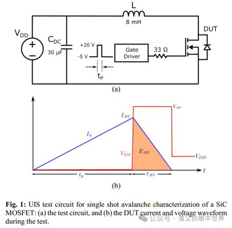
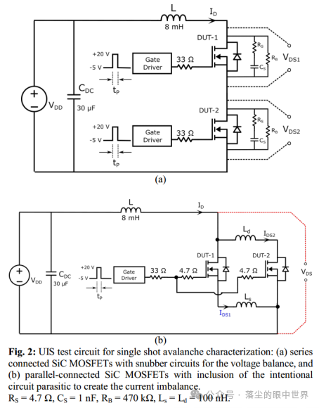
Fig. 2(a) shows the UIS test circuit for the avalanche characterization of series-connected SiC MOSFETs. Two medium voltage gate drivers were used to drive the two DUTs separately. A passive RC snubber based voltage balancing circuit was connected across each of the two DUTs to minimize the voltage imbalance during the test [2]. The test circuit was operated in the similar manner as shown in Fig.
1(b). High bandwidth 6kV, 100 MHz differential voltage probes were used to measure the DUT drain-to-source voltage in the series connection.
图2(a)显示了用于串联SiC MOSFET雪崩特性的UIS测试电路。两个中压栅极驱动器分别驱动两个DUT。在两个被试之间分别连接了一个基于无源RC缓冲器的电压平衡电路,以尽量减少测试期间的电压不平衡[2]。测试电路的操作方法与图1(b)所示相似。采用高带宽6kV,100mhz差分电压探头,测量被测件漏源电压。
Fig. 2(b) shows the UIS test circuit for the parallel
connected SiC MOSFETs. A single gate driver with its own isolated dc-dc converter was used to drive the two parallel MOSFETs with an external gate resistor of 33Ω. An internal gate resistor of 4.7Ω was connected in series to the gate of each of the MOSFETs. The UIS test was performed with an intentional current imbalance in the parallel connection to observe the effect of the current mismatch on the avalanche behavior. Two wire strips having approximate inductance of 100nH were introduced in the drain and in the source path of the DUTs, shown as Ld and Ls
in Fig. 2(b).
图2(b)显示了平行连接SiC MOSFET的UIS测试电路。采用带有隔离DC-DC变换器的单栅驱动器驱动两个具有33Ω外部栅极电阻的并联MOSFET。内部栅极电阻4.7Ω串联到每个MOSFET的栅极上。UIS测试是在并联中故意设置电流不平衡的情况下进行的,以观察电流不匹配对雪崩行为的影响。在DUT的漏极和源极路径中引入两条电感近似为100nH的导线带,如图2(b)中的Ld和Ls所示。
Ⅲ. Results And Discussion
In this work, 1700V, 40A SiC power MOSFETs were used for the avalanche characterization in series and parallel connection [12]. First, the 1700V MOSFET was characterized in single operation using the UIS test circuit to determine its critical single shot avalanche energy. Thereafter, the MOSFETs were tested in the series and parallel connection separately. A gate drive voltage of +20V/-5V were employed for switching of the DUTs. New 1700V MOSFETs were used in all the tests. All the tests were performed at room temperature.
在本工作中,使用1700V、40A SiC功率MOSFET在串并联连接[12]中进行雪崩表征。首先,使用UIS测试电路对1700V MOSFET进行单次工作表征,以确定其临界单次雪崩能量。然后,分别在串联和并联中测试了MOSFET。采用+20V/-5V的栅极驱动电压进行被测器件的开关。所有测试均采用新型1700V MOSFET。所有试验均在室温下进行。
A. Single MOSFET
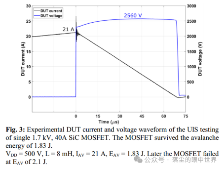
The 1700 V SiC MOSFET was tested using the circuit shown in Fig. 1(a) in the single shot operation. An air core inductor of 8mH was connected in the circuit to store the avalanche energy before dissipating into the DUT. Fig. 3 shows the experimental waveform of the MOSFET drain-to-source voltage and the drain current. The MOSFET dissipated total avalanche energy of 1.83J at the peak current of 21A without a failure. In the subsequent experiment, the MOSFET failed at total avalanche energy of 2.1J.
1700 V SiC MOSFET使用图1(a)所示的电路在单次操作中进行测试。电路中连接了一个8mH的空芯电感,在雪崩能量消散到被测设备之前存储雪崩能量。图3显示了MOSFET漏极源极电压和漏极电流的实验波形。在峰值电流为21A时,MOSFET消耗了1.83J的总雪崩能量而没有发生故障。在随后的实验中,MOSFET在总雪崩能量为2.1J时失效。
B. Series Connected MOSFETs
Before subjecting the series-connected 1700 V MOSFETs to avalanche condition, a passive RC snubber network was designed and tested for static and dynamic voltage balancing.
RB was selected based on the leakage current values of the two MOSFETs at room temperature. The dynamic balancing network Rs-Cs were selected based on the threshold voltage difference of the MOSFETs along with the inherent delays associated with the individual gate drive channels.
在将串联的1700 V MOSFET置于雪崩状态之前,设计了无源RC缓冲网络,并对其进行了静态和动态电压平衡测试。根据两个MOSFET在室温下的泄漏电流值选择RB。根据MOSFET的阈值电压差以及与各个栅极驱动通道相关的固有延迟来选择动态平衡网络RS-CS。
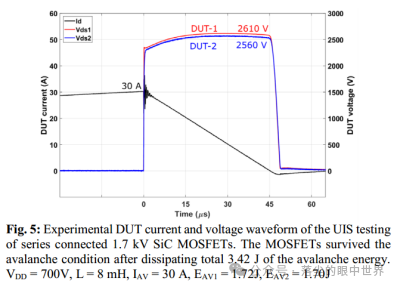
Fig. 4 shows the photograph of the experimental setup for UIS test of the series-connected MOSFETs. Fig. 5 shows the experimental results at total energy of 3.42 J for the series connected MOSFETs without a failure. Both the MOSFETs survived after dissipating 1.72 J and 1.70 J of the avalanche energy. During the avalanche condition, both the MOSFETs were showing approximately equal avalanche voltage.
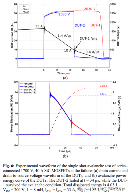
Thereafter, peak current of the inductor L was increased so that total 4.03 J of the avalanche energy was dissipated in the DUTs. Fig. 6 shows the experimental results in that operating condition. The DUT-2 failed at the avalanche energy of 1.83 J, while the DUT-1 survived even after dissipating a higher avalanche energy of 2.20 J.
图4显示了串联MOSFET的UIS测试实验装置的照片。图5显示了在总能量为3.42J时串联MOSFET未失效的实验结果。在消耗了1.72J和1.70J的雪崩能量后,两个MOSFET都存活了下来。在雪崩条件下,两个MOSFET显示出近似相等的雪崩电压。此后,电感器L的峰值电流增加,使得雪崩能量在被测件中总共耗散了4.03J。图6为该工况下的实验结果。DUT-2在1.83J的雪崩能量下失效,而DUT-1在消耗更高的2.20J的雪崩能量后仍然存活。

C. Parallel Connected MOSFETs
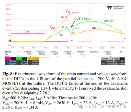
There is a natural imbalance in the current distribution when two MOSFETs are connected in parallel due to mismatch in the transfer characteristics and the asymmetric parasitic layout in the power and control circuits. For the single shot avalanche characterization of parallel-connected MOSFETs, two 1700 V, 40 A SiC MOSFETs were used with same internal gate resistors. A common gate drive channel was connected in series with an external gate resistor to drive the two parallel MOSFETs. Fig. 7 shows the experimental waveform at total peak current of 30 A and avalanche energy of 4.05 J without a failure. Fig. 7(a) shows the drain current and drain-to-source voltage waveform of the DUTs without a failure. There was an initial imbalance of 10 A in the DUT currents before start of the avalanche event. Power-energy curve of the DUTs are shown in Fig. 7(b). Current and voltage waveform of the DUTs are zoomed-in at the start of the avalanche event, and shown in Fig. 7(c). DUT-2 was carrying the lower share of the total current before start of the avalanche event. Immediately after the DUTs went into avalanche, the DUT-2 switched to carry the higher current, which later started carrying the lower share of the total avalanche current after 1.3 µs as shown in Fig. 7(c). The dissipated avalanche energy in the DUT-1 was higher compared to that in the DUT-2, owing to the higher share of the total current before and during the avalanche condition for most of the time duration.
当两个MOSFET并联时,由于传输特性的不匹配以及电源和控制电路中的不对称寄生布局,会导致电流分布的自然不平衡。对于并联MOSFET的单次雪崩特性,两个1700 V、40 A的SiC MOSFET使用相同的内部栅极电阻。一个公共栅极驱动通道与一个外部栅极电阻串联,以驱动两个并联的MOSFET。图7为总峰值电流为30A,雪崩能量为4.05J时无故障的实验波形。图7(a)显示了无故障DUT的漏极电流和漏源电压波形。在雪崩事件开始之前,DUT电流存在10 A的初始不平衡。被测件的功率-能量曲线如图7(b)所示。雪崩事件开始时被试的电流和电压波形放大,如图7(c)所示。在雪崩事件发生前,DUT-2携带的总电流份额较低。如图7(c)所示,在DUT进入雪崩状态后,DUT-2立即切换为携带较大电流,随后在1.3µs后,DUT-2开始携带雪崩总电流的较低份额。DUT-1的雪崩耗散能量高于DUT-2,这是由于在雪崩发生前和雪崩发生期间的大部分时间内,总电流所占的份额更高。
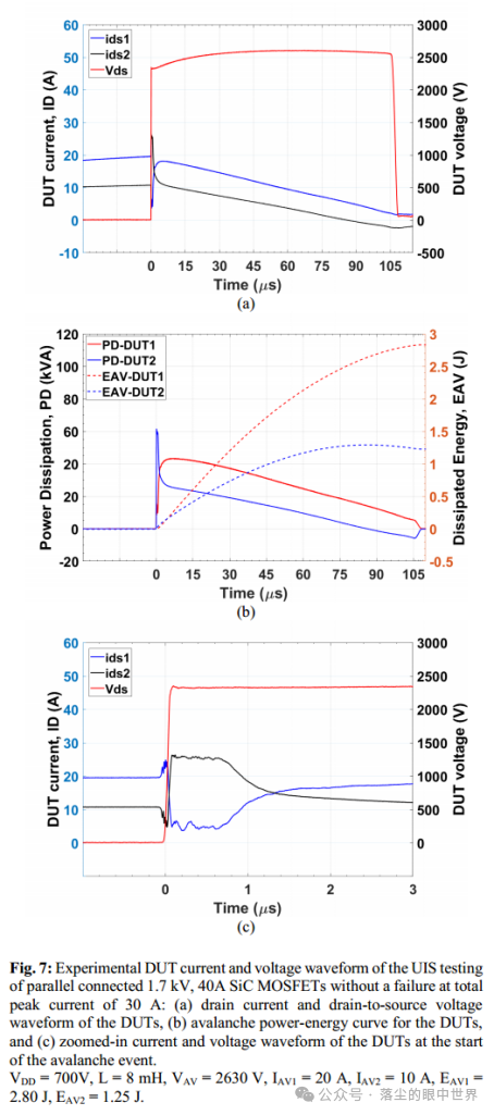
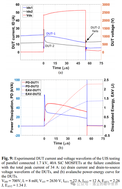
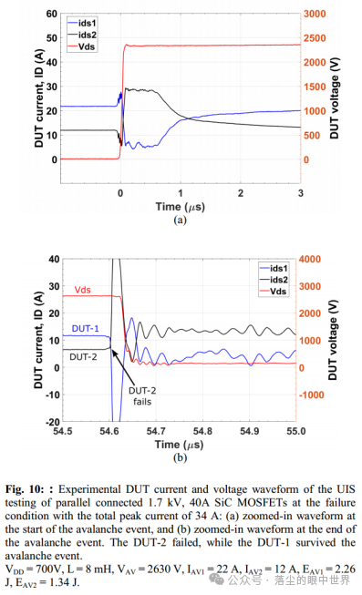
Total avalanche energy of the UIS test circuit was increased later using the same pair of the DUTs to observe the failure. Fig. 8 shows the experimental drain current and voltage waveform of the DUTs before and after the avalanche event. The DUT-2 failed after dissipating 1.34 J, while the DUT-1 survived the avalanche condition even after dissipating higher avalanche energy of 2.26 J. Fig. 9(a) shows the experimental current and voltage waveform of the DUTs during the avalanche condition. Avalanche power-energy curve of the DUTs are shown in Fig. 9(b). Zoomed-in version of the drain current and voltage waveform of the DUTs at the start and the end of the avalanche event are shown in Fig. 10.
The DUT-1 was carrying higher share of the total current before start of the avalanche event. When the avalanche starts, the DUT-2 took higher share of the current, and again started taking lower share of the current after 1.1 µs. At the end of the avalanche event, the DUT-2 current jumped up, and eventually failed as shown in Fig. 10(b).
随后使用同一对DUT观察失效,增加了UIS测试电路的总雪崩能量。图8为雪崩事件前后被测件实验漏极电流和电压波形。DUT-2在耗散1.34J后失效,而DUT-1在耗散更高的雪崩能量2.26J后幸存下来。图9(a)为雪崩条件下DUT的实验电流和电压波形。被试雪崩功率-能量曲线如图9(b)所示。雪崩事件开始和结束时被试漏极电流和电压波形的放大版本如图10所示。在雪崩事件发生前,DUT-1携带的总电流份额较高。雪崩开始时,DUT-2的电流占比较高,1.1µs后,DUT-2的电流占比又开始下降。雪崩事件结束时,DUT-2电流跳升,最终失效,如图10(b)所示。
Ⅳ. Conclusion
Prior works have documented the avalanche ruggedness of single SiC MOSFETs and their failure mechanism. This is the first study to our knowledge to investigate the single shot avalanche ruggedness of series-connected SiC power MOSFETs. In this study we tested the single shot avalanche ruggedness of series and parallel-connected 1700 V SiC power MOSFETs using conventional UIS test circuit. First, the critical avalanche energy of the single SiC MOSFET was determined by the UIS test circuit to be 2.1 J. During the avalanche failure tests of both the series-connected and the parallel-connected MOSFETs, only one of the MOSFETs failed which had dissipated lower amount of the avalanche energy. The series-combination failed at the total avalanche energy of 4.03 J, while it took 3.60 J of total avalanche energy for the parallel combination of the MOSFETs to fail. In the parallel connected MOSFETs, the slower MOSFET failed which was carrying the lower share of the current. Future work should include the device physics based analysis to explain the failure of the MOSFET with lower share of the current in the parallel combination. Also, there remains a need to explain the failure of the MOSFETs with lower dissipated avalanche energy in both the series connection and the parallel connection.
先前的工作已经记录了单SiC MOSFET的雪崩坚固性及其失效机制。据我们所知,这是第一次研究串联SiC功率MOSFET的单次雪崩坚固性。在本研究中,我们使用传统的UIS测试电路测试了1700V SiC功率MOSFET串联和并联的单次雪崩坚固性。首先,UIS测试电路确定单SiC MOSFET的临界雪崩能量为2.1J。在串联和并联MOSFET的雪崩失效测试中,只有一个MOSFET损耗了较低的雪崩能量。串联组合在总雪崩能量为4.03J时失败,而并联组合在总雪崩能量为3.60 J时失败。在并联的MOSFET中,承载较低电流份额的较慢的MOSFET失效。未来的工作应该包括基于器件物理的分析,以解释在并联组合中具有较低电流份额的MOSFET的故障。此外,仍然需要解释在串联连接和并联连接中具有较低损耗雪崩能量的MOSFET的失效。
-- End --
原文始发于微信公众号(易矽科技):2024.11.12文献阅读——SiC功率MOSFET串、并联的单次雪崩特性

